Tantalum Products | Refractory Metal
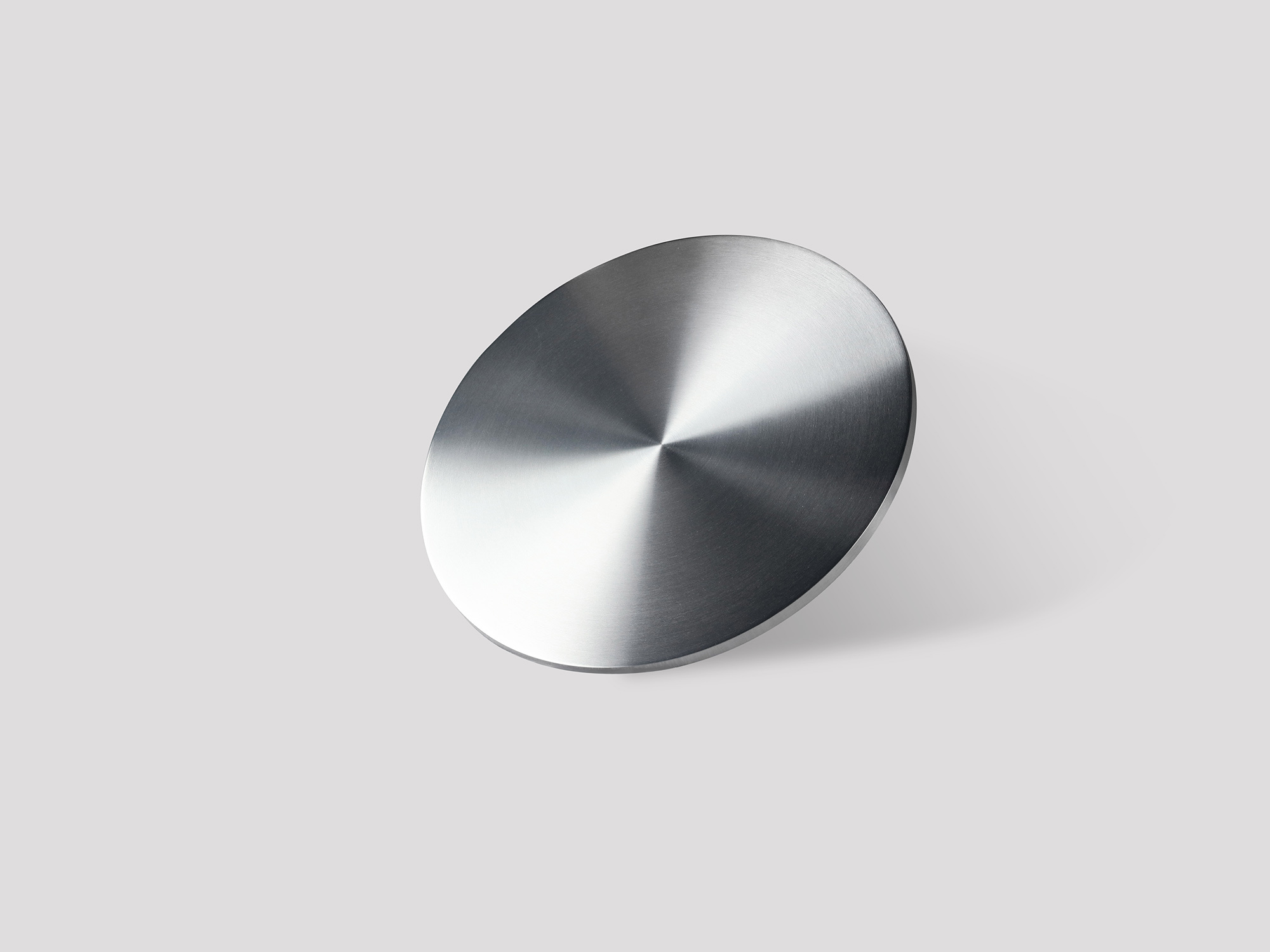
Tantalum Target Material
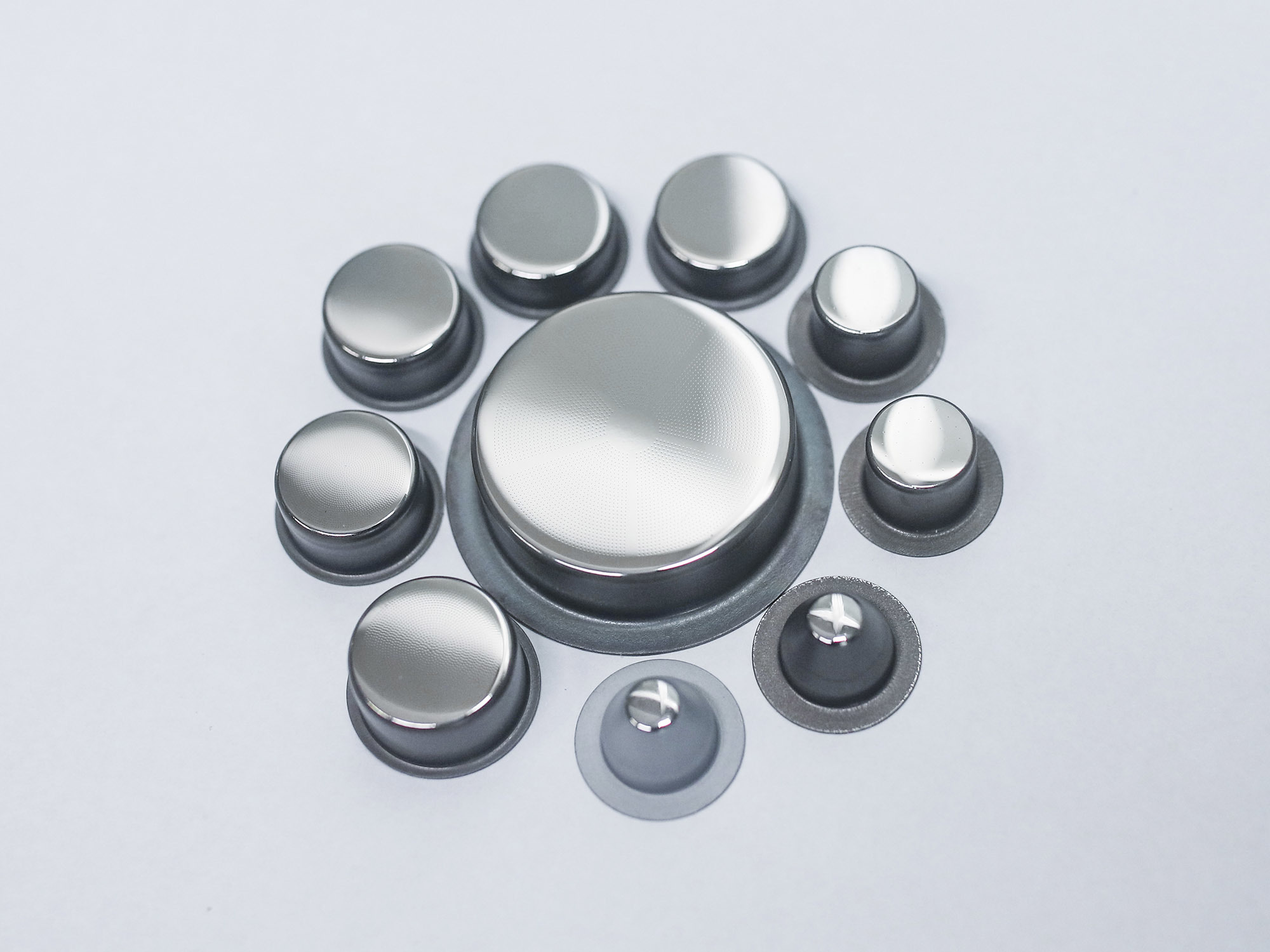
High-purity tantalum sputtering targets for thin film deposition in semiconductor, optical, and decorative coating applications. Available as planar targets, rotary targets, and custom geometries with purity levels from 99.95% to 99.999%. Our tantalum targets feature uniform grain structure, controlled crystallographic orientation, and excellent bonding quality for consistent sputtering performance and long target life. Essential for semiconductor barrier layers, optical coatings, hard disk media, and architectural glass coatings.
✅ Customized-made is available
About Tantalum Target Material
Our tantalum sputtering targets are manufactured from high-purity tantalum through powder metallurgy or electron beam melting, followed by precision machining and surface finishing. Each target is characterized for purity, grain size, crystallographic orientation, and density to ensure optimal sputtering performance.
Features
- Purity: 99.95% to 99.999%
- Planar and rotary target geometries
- Uniform grain structure
- Controlled crystallographic orientation
- Excellent bonding quality
- Consistent sputtering rates
- Long target life
- Custom sizes and shapes
- Indium bonding or elastomer bonding
- Full characterization report
Specifications
| Material | Tantalum (Ta) |
|---|---|
| Purity | 99.95% - 99.999% |
| Target Types | Planar, rotary, custom |
| Sizes | Up to 500mm diameter, 2000mm length (rotary) |
| Grain Size | <100μm (standard), <50μm (fine grain) |
| Crystal Orientation | Random or textured |
| Bonding | Indium, elastomer, or mechanical |
| Density | ≥99.5% theoretical |
| Surface Roughness | Ra ≤ 0.5μm |
| Packaging | Clean room packed, vacuum sealed |
How Tantalum Sputtering Targets are Manufactured — Production Process
Our tantalum sputtering targets are manufactured through a precision powder metallurgy and thermomechanical processing route that achieves the ultra-high purity, fine grain structure, and crystallographic texture control required for consistent thin-film deposition in semiconductor and optical coating applications.
Production begins with high-purity tantalum powder (≥99.99%) that is cold isostatic pressed (CIP) into green compacts. The compacts are then sintered in vacuum at 2000–2400°C to achieve near-full density (>99.5% theoretical density). The sintered billet undergoes hot isostatic pressing (HIP) to close residual porosity and achieve full density, followed by hot forging and rolling to develop the required grain structure and crystallographic texture.
Final processing includes precision machining to exact dimensional specifications, surface polishing to achieve the required surface roughness (Ra ≤0.4μm), and bonding to backing plates using indium solder or electron beam welding. Each target undergoes chemical analysis (GDMS), grain size measurement (ASTM E112), texture analysis (XRD), and ultrasonic inspection for bonding integrity.
Applications of Tantalum Sputtering Targets
Tantalum sputtering targets are essential components in thin-film deposition processes across multiple high-technology industries:
Semiconductor Barrier Layers
Tantalum and tantalum nitride thin films serve as critical barrier layers in copper interconnect technology, preventing copper diffusion into silicon dioxide dielectric layers. Tantalum sputtering targets are used in every advanced semiconductor fabrication facility worldwide for depositing these barrier layers at the 7nm node and below.
Optical Coatings
Tantalum thin films are deposited as high-index layers in optical interference coatings for lenses, mirrors, filters, and display panels. The material's high refractive index and chemical stability produce durable optical coatings with excellent spectral performance.
Hard Coatings for Cutting Tools
Tantalum nitride coatings deposited from tantalum targets provide exceptional hardness, wear resistance, and chemical inertness for cutting tools, drill bits, and forming dies. These coatings extend tool life by 3–10x in aggressive machining applications.
Flat Panel Display Manufacturing
Tantalum sputtering targets are used in the deposition of thin-film transistors (TFTs) and interconnect layers in LCD and OLED display manufacturing. The targets' purity and uniformity ensure consistent electrical properties across large glass substrates.
Frequently Asked Questions about Tantalum Target Material
Q: What purity levels are available for tantalum targets?
A: We offer tantalum sputtering targets in 99.95%, 99.99%, 99.995%, and 99.999% purity levels. Higher purity is specified for semiconductor and advanced electronics applications.
Q: What target geometries do you manufacture?
A: We produce planar (flat) targets, rotary (cylindrical) targets, and custom geometries including annular, disc, and irregular shapes to fit specific PVD chamber configurations.
Q: How do you ensure uniform sputtering?
A: We control grain size (<100μm standard), crystallographic orientation (random or textured), and porosity (<0.5%) to ensure uniform erosion and consistent thin film properties throughout target life.
Q: What bonding methods are available?
A: We offer indium bonding (best thermal conductivity), elastomer bonding (for thermal cycling), and mechanical clamping. Indium bonding is recommended for most applications.
Q: What applications use tantalum sputtering targets?
A: Primary applications include semiconductor diffusion barriers (TaN/Ta), optical coatings, hard disk media, decorative coatings, and wear-resistant tool coatings. Tantalum provides excellent barrier properties and adhesion.